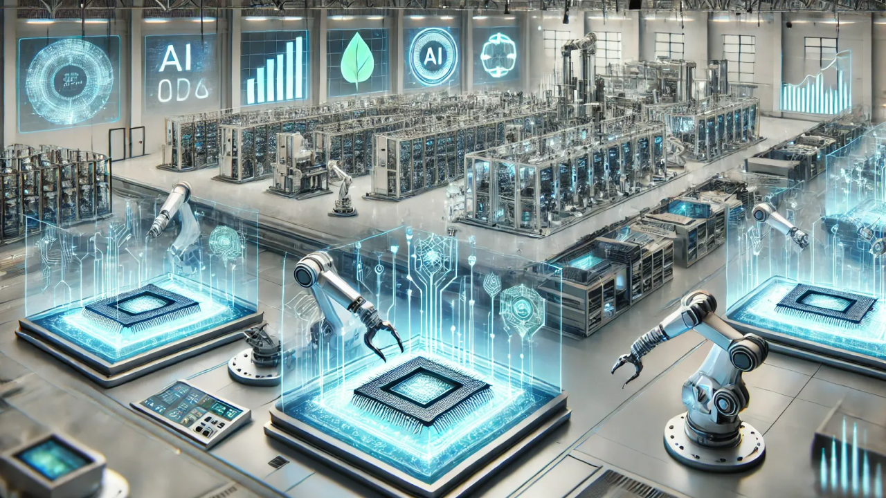
AI-Driven Material Simulations: Cutting R&D Costs in Semiconductor Innovation
Developing new semiconductor materials has always been a costly and time-intensive endeavor. Traditional research and development rely heavily on laboratory experiments that demand expensive equipment, rare materials, and months, sometimes years, of testing. Erik Hosler, a semiconductor innovation expert, highlights how AI-driven simulations are accelerating breakthroughs while significantly lowering research costs. As the industry pushes beyond silicon toward alternatives like gallium nitride, silicon carbide, and novel 2D compounds, the stakes have only grown higher. Artificial Intelligence (AI) is transforming this process by enabling advanced material simulations that reduce the need for costly physical experiments.
This shift is arriving at a critical time. Demand for faster, smaller, and more energy-efficient chips continues to surge across artificial intelligence, automotive, and consumer electronics sectors. Traditional R&D models cannot keep pace with this accelerating demand, nor can companies afford the ballooning costs of trial-and-error experimentation. AI-powered simulations offer a way forward, using data-driven models to replicate, predict, and optimize material behavior virtually. By reducing reliance on physical prototyping, these tools cut costs while speeding up the discovery-to-application pipeline.
Why Traditional R&D Is So Expensive
The search for new semiconductor materials has historically depended on iterative experiments. Scientists synthesize candidate compounds, test their properties, refine compositions, and repeat the cycle. Each step requires specialized equipment, precise environmental controls, and considerable time investments.
The costs add up quickly. Rare elements and fabrication processes make each experiment expensive, while failed tests still consume valuable resources. A single fabrication run may cost hundreds of thousands of dollars, yet deliver little usable insight if the material proves unstable. Moreover, scaling successful experiments to production introduces additional rounds of testing, further inflating R&D budgets. This reality makes innovation prohibitively slow and expensive for many fabs, forcing them to prioritize only the safest bets rather than more experimental avenues.
How AI Changes the R&D Equation
Artificial intelligence improves this model by computationally simulating material behavior. Machine learning algorithms trained on vast libraries of experimental data can predict how new compounds will perform without requiring immediate physical synthesis. These simulations account for structural, electronic, and thermal properties, allowing researchers to evaluate performance virtually.
This approach dramatically reduces costs. Instead of running thousands of lab experiments, researchers can narrow down to a handful of the most promising candidates for real-world testing. In many cases, simulations that once required supercomputers can now be run on advanced cloud platforms, making the economics even more attractive. The result is a faster, more efficient pipeline where resources are concentrated where they matter most.
Accelerating Discovery Through Simulation
AI-driven simulations go beyond screening. They allow scientists to model how materials behave under realistic operating conditions, such as elevated temperatures, electrical stress, or nanoscale confinement. Such simulations reveal potential weaknesses before costly prototypes are built.
For example, carbon nanotube transistors can be simulated under different strain conditions to predict how they affect electron mobility. Similarly, perovskites can be modeled under varied environmental stresses to test long-term stability. These insights accelerate discovery while reducing the risks associated with investing in new material development.
In addition, AI enables multi-objective optimization, balancing trade-offs between performance, cost, and sustainability. Researchers can simulate not just how a material performs but also how it aligns with environmental goals and economic feasibility, something that traditional lab-first approaches rarely account for at the initial stages.
Precision Insights and Predictive Power
The strength of AI simulations lies in their ability to uncover subtle correlations that human researchers might overlook. By analyzing large datasets, AI can reveal how microscopic structural differences translate into macroscopic performance. This precision guides researchers in refining materials with greater accuracy.
The predictive power of AI ensures that failures happen in silico rather than in the lab. Each avoided failed experiment represents cost savings and accelerates the overall pace of innovation. In this way, AI becomes a multiplier of human expertise, enhancing scientific discovery while conserving resources.
Scaling From Lab to Fab
The real test for any new semiconductor material is whether it can be scaled from the lab to mass production. AI simulations support this transition by modeling how materials interact with existing fabrication processes. They help identify potential bottlenecks, such as compatibility issues with lithography or deposition techniques, before production begins.
By anticipating these challenges, fabs can adjust workflows and equipment configurations proactively. This foresight reduces delays and ensures that promising materials move smoothly from discovery to commercialization. It also minimizes the risk of costly surprises during pilot production, where delays can mean millions in lost opportunities.
From Experimentation to Innovation
Industry is increasingly recognizing that AI-driven simulations are more than a cost-saving tool. They are drivers of innovation. By compressing development timelines, they allow researchers to explore bolder material candidates that might otherwise be too expensive or risky to pursue.
Erik Hosler emphasizes, “Working with new materials like GaN and SiC is unlocking new potential in semiconductor fabrication. Accelerator technologies provide the tools needed to develop these materials at scale.” His perspective illustrates how AI not only reduces costs but also expands the scope of exploration, making ambitious breakthroughs achievable.
Barriers to Adoption
Despite their advantages, AI-driven simulations face challenges. Building accurate predictive models requires high-quality training datasets, which may be limited to emerging research. Validation is also necessary. AI predictions must be confirmed experimentally, ensuring accuracy before results are applied at scale.
Integrating AI into established R&D workflows requires cultural shifts. Researchers accustomed to traditional experimentation may be hesitant to trust computational models. Interdisciplinary collaboration is critical, requiring chemists, physicists, and computer scientists to work seamlessly together. Transparency and explainability of AI outputs will be essential for broader adoption, giving engineers confidence that simulations can be relied upon for high-stakes decisions.
Pioneering a Smarter Path to Discovery
AI-driven material simulations represent a turning point in semiconductor R&D. By reducing reliance on costly experiments, these tools lower barriers to innovation, speed up discovery, and expand the possibilities for next-generation semiconductors. They are not just about saving money, but enabling the latest ideas that would once have been impossible to test.
As the industry continues its search for materials beyond silicon, AI-powered simulations will become an essential part of the innovation toolkit. Those who adopt them early will not only save resources but also pioneer a smarter, faster path to discovery, shaping the materials that will define the future of electronics. In doing so, they are not simply cutting costs, but redefining how the industry approaches research itself.


